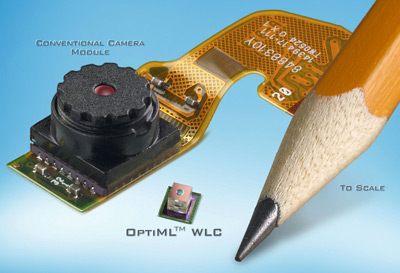
Chip-packaging company Tessera Technologies Inc. unveiled a technology today (June 11) that makes it possible to manufacture thousands of lenses simultaneously on a semiconductor wafer. Lenses aligned and bonded at the wafer level and assembled into optical elements are then attached to an image sensor at the die level.
Tessera (San Jose, Calif.) claims its technology, available for licensing as intellectual property, reduces optical-module size by 50 percent over today's camera modules for cell phones.

While handsets keep shrinking, camera phone optics traditionally "don't scale well," said Mike Feldman, CTO at Tessera. More problematic is that optical elements usually require a higher-level alignment procedure, and conventional cameras don't survive reflow.
Teserra's OptiML WLC technology promises scalability with pixel size as well as reflow compatibility. The process of aligning and bonding the lenses at the wafer level eliminates the need for costly manual focusing. The optical elements use reflow-compatible materials and are available in both wirebond and BGA formats. When BGA is used, the optical element can be directly placed on a board.
All told, the OptiML WLC technology enables up to a 30 percent reduction in cost for camera module manufacturers, according to Feldman.
He said the new optical element, which eliminates such parts as plastic molds and flex-lead cables, has an X-Y dimension smaller than that of a sensor chip. As for height—usually a challenge for camera modules—Tessera claims the "Z" dimension for the OptiML WLC's VGA implementation comes in at 2.5 mm. Conventional modules range from 3.5 mm to more than 5 mm, according to the company.
For Tessera, whose core business thus far has been IC packaging for chips and memory, the OptiML WLC technology represents an opportunity to expand its technology portfolio into consumer optics. Indeed, over the past 18 months, Tessera has been on a shopping spree in the sector, having picked up wafer-level-packaging expert Shellcase Ltd. (Jerusalem); Digital Optics Corp. (Charlotte, N.C.), a specialist in wafer-level micro-optics technology; and Eyesquad (Tel Aviv, Israel), which has autofocus and optical-zoom expertise.
Shellcase provides wafer-level packaging for both surface-mount and wirebond cameras. Digital Optics applies microelectronics techniques to optics, allowing production of well-aligned lenses on wafers.
Eyesquad's digital focus technology becomes crucial when wafer-level cameras need 2-megapixel resolution or better. Its advanced autofocus and digital zoom are said to offer depth-of-field for higher-resolution cameras without using moving parts.
Making cameras on the wafer level has been an R&D priority for both conventional digital-camera manufacturers and image sensor suppliers. "Different companies are working on different pieces, but nobody has yet put together the whole thing available for licensing," said Feldman.
While declining to name potential customers, Feldman said, "We are in active discussions with key members in the [camera phone] supply chain."
The first working-prototype module made to custom specs using OptiML WLC will emerge at the end of next quarter, according to Tessera's Feldman. Wafer-level cameras will be incorporated in handsets by the end of 2008, he predicted.
Copyright © 2006 CMP Media LLC , EETimes EU Copyright. All rights reserved. To subscribe or visit go to: http://www.eetimes.eu