Solar-cell technologies promise higher efficiency
New technologies may reduce PV cost/watt by a factor of 2 to 3
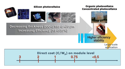
The European Photovoltaic Industry Association (EPIA) foresees a share of PV-generated electricity above 10% in 2020. But, this is only feasible if the cost of the photovoltaic systems (around €4/W for an industrial system) can be reduced by a factor of 2 to 3, and this will require some technological breakthroughs. In this article, four photovoltaic technologies are discussed in view of these objectives: crystalline Si solar cells, organic solar cells, concentrators and thermophotovoltaic cells.
There are other mature solar-cell concepts studied worldwide, such as amorphous-Si-based solar cells, II-VI-based solar cells (CIGS or CdTe), or dye-sensitized solar cells, as well as some exploratory concepts, generally described by the term “third-generation PV-concepts,” which will not be covered here.
Si-based photovoltaics
The present PV market is dominated by crystalline Si solar cells, with a world market share of 85% in 2008. This dominance is expected to continue for at least the next decade. About 50% of the cost of present Si PV modules is in the expensive electronic-grade Si, and the main road being followed is to reduce the thickness of the Si wafers. In 2004, the standard thickness in industry was still near 300 µm, it was 200 µm in 2008, and 180 µm is likely to become generally used in 2009. This trend will probably continue.

Besides cost reduction, a commercially viable PV system calls for improved efficiency to 18% to 20%, instead of the current 14% to 15%, and the reliability needs improvement to garner guaranteed lifetimes of near 35 years.
Thin wafer-based crystalline Si solar cells
Realization of Si solar cells on very thin substrates can only happen if there is progress in wafer-handling and solar-cell process technology. In previous years, IMEC introduced the i-PERC process that allows thin-wafer manufacturing. This concept has become well-known and is presently being introduced in the industry. Passivated emitter and rear cell (PERC) technology features passivation of the rear surface by a dielectric and point rear contacts. Today, 80-µm thin monocrystalline Si solar cells can be made with a large surface (200 cm2) and with efficiencies of more than 16.6%.
Another concept is the i-PERL (passivated emitter, rear locally diffused) cell that can be used for the fabrication of small-area high-efficiency solar cells, with 1-sun efficiencies of nearly 25%. In the i2-BC (industrial interdigitated back-contact) solar-cell concept, the front-surface metal grid is removed for a higher effective area. It also, potentially, allows for significant cost reductions in assembly. Finally, the U-cell, or ultra-thin bulk Si solar cell, has wafers as thin as 40 µm and requires innovative production methods. IMEC recently presented a novel technique that does not require expensive implanters and uses a “lift-off” process, and requires only the use of a screen-printer and a belt furnace.
Thin-film crystalline Si solar cells
In the epi-cell concept, epitaxial thin-film solar cells are made by growing a thin high-quality active layer of Si (20 µm) on top of a low-cost highly doped crystalline Si wafer. This reduces material cost, and, as the solar-cell process is similar to a classical bulk Si process, it is easy to implement in existing production lines. In a thin-film Si solar-cell approach, nonsilicon substrates are also being pursued.
Organic solar cells
Organic solar cells have a larger absorption coefficient than crystalline Si, where light has to travel a long way before it is absorbed. The active layers of organic solar cells are 100 nm to several microns thick. The low material consumption and the fact that methods used to deposit these layers (printing) are compatible with extremely high production throughputs (1 or 2 orders of magnitude better than present technologies), could result in costs reductions of a factor 5 to 10. But, at least for now, they are not efficient enough, at only about 6% for the best in the laboratory. Nevertheless, they can today be used in some niche applications where the low efficiency is acceptable.

One of the most promising concepts in the field of organic solar cells is that of the bulk donor/acceptor heterojunction, where the active layer consists of a mixture of two conjugated organic materials sandwiched between metallic electrodes. Investigations of this device concept focus along two main routes. The first considers polymer-based organic cells in which the active layer can be processed from solution. Typically, spin coating is used and efficiencies above 5% could be realized. Successful steps have also been made toward the introduction of airbrush spray coating and of a printing technology like screen printing. Secondly, active organic layers can be deposited by vacuum evaporation. PV stability improvements are being obtained by new methods and conjugated polymers that stabilize the nanomorphology of the active layer.
Concentrators
Very high efficiencies can be obtained when sun light is first concentrated with mirrors or lenses, before it is absorbed by a solar cell. The semiconductors can be chosen to absorb nearly the entire solar spectrum. The state-of-the-art triple-junction InGaP/(In)GaAs/Ge monolithic stacks hold a world record efficiency of 40%. IMEC is also researching the stacking of independent subcells, capable of conversion efficiencies 1-2% higher than the triple-junction cells.
Thermophotovoltaic cells
TPV devices place photovoltaic cells in close proximity to a combustion heat source (usually 1,340° to 2,420°F). TPV generators are very simple and can be very small. The most significant difference between TPV and conventional solar PV cells is the use of low-bandgap materials to exploit low energy, long wavelength IR photons. Silicon cells are not effective here because most thermal radiation falls short of their bandgap (silicon Eg = 1.12 eV).
Several low-bandgap III-V compounds are being investigated in a number of institutes worldwide. IMEC is looking at using high-efficiency, low-bandgap germanium cells and has recently shown cells with an improved surface passivation technique and novel contacting technologies. Ge is low cost, relative to III-V compound alternatives.