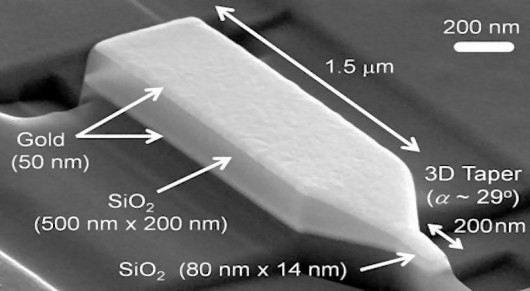
Engineers at the California Institute of Technology (CalTech) and the University of California at Berkeley have developed a nanofocusing waveguide, a tiny passive plasmonic device which is capable of concentrating light onto a spot a few nanometers in size. In so doing, they have sidestepped the diffraction-limited nature of light, which normally prevents focusing light to a spot smaller than its own wavelength. This remarkable feat may lead to new optoelectronic applications in computing, communications, and imaging.
Light can carry data more efficiently than is possible using pulses of electrons in wires. Encoding data into optical pulses can often result in faster logic and smaller energy consumption than is possible using semiconductor logic alone. As a result, today's technology is increasingly being pulled toward optoelectronics, the study and application of electronic devices that source, detect and control light.
Ideally, methods would be found to efficiently couple light to individual transistors. However, light can only be directed onto a spot roughly equal to the light's wavelength – in practice between half a micron and a couple of microns. As transistors on current integrated circuits are about 40-50 nm in size, the result is an intolerable mismatch that leads to poor optical sensitivity and quantum efficiency.
One way to focus light into tinier spaces is to reduce its wavelength by slowing the light. There are a number of techniques for slowing light itself by manipulating the dielectric constant of a material through which the light is passing. For example, electromagnetically induced transparency can give an optical medium the desired properties, and a medium in which light travels very slowly can be made of a Bose-Einstein condensate. However, these methods are not currently practical for high-density integrated optoelectronics.
The CalTech/Berkeley research team, co-led by Prof. Hyuck Choo of CalTech and Prof. Eli Yablonovitch of UC-Berkeley, uses plasmonics to achieve the goal of smaller wavelength "light." When a photon is combined with electron plasma oscillations which occur naturally at a metal surface, a surface plasmon polariton (SPP) is formed. An SPP has the same frequency of oscillation as did the photon, but travels slowly along the metal surface, giving the SPP a wavelength far smaller than that of the photon.
The new nanofocusing waveguide is a tapered structure made of silica glass covered by a thin layer of gold. This device transforms light into SPPs, and then concentrates the SPPs into a region only a few nm across, producing energy densities thousands of times larger than could be accomplished using light alone.
CalTech's new nanofocusing plasmonic waveguide is a tapered silica glass structure covered with a thin layer of gold
As light is sent through the waveguide, the photons interact with electrons at the interface between the gold and the silicon dioxide. Those electrons oscillate, forming SPPs that travel along the device as waves which are more similar to sound waves than to light waves. However, because the electron oscillations are coupled to the light, they carry the same information and properties (even to the extent of preserving quantum entanglement relations). The waveguide then focuses the SPPs as they travel toward the pointed end. When the SPPs reach the pointed end, they can directly excite target structures through direct interaction of the SPPs, or by the SPPs escaping from the waveguide and reconverting into light. As you can observe in the video below, nanofocusing waveguides can be easily built on a semiconductor chip.
The CalTech/Berkeley nanofocusing waveguide can produce a point of light only a few nm in size, with roughly 50 percent optical efficiency, meaning that half the incoming photons are converted into SPPs that are focused into the nm-sized point of light. The key feature behind the device's focusing ability and efficiency is its unique design and shape. This is a situation where having the basic concept is nice, but the devil is in the details – high performance requires balancing delicate interactions among the various phenomena occurring in this deceptively simple appearing plasmonic element.
While the obvious application for the nanofocusing waveguide is to boost the resolution of near-field scanning optical microscopy from 20 nm to five nm, there are potential applications which would have more impact. One near-term application for this new technology is in heat-assisted magnetic recording.
A hard drive stores data in rows of tiny magnets whose magnetic poles can be switched by applying a magnetic field. However, when the magnetic bit becomes too small, a magnetic field cannot be simultaneously focused to just affect one bit while at the same time providing a strong enough magnetic field to change the polarity of that bit. As a result, conventional hard disks will be hard put to break the terabit per square inch barrier (155 Gb per square cm).
In heat-assisted magnetic recording (HAMR), a laser pulse heats a single magnetic bit enough that its magnetic polarity can be changed by an applied magnetic field. This allows magnetic bits to be the size of a region that can be quickly and reliably heated and cooled. A nanofocusing waveguide can heat magnetic bits as small as a few nm, compared to about 300 nm for direct laser light. The corresponding data storage density should be around 50 terabits per square inch (eight terabits per square cm.)
The nanofocusing waveguide may enable a host of other applications, some (but potentially not all) of which may be welcome improvements. What is important at this time is that this very important door has been opened.
The following video shows a nanofocusing waveguide being fabricated. A high-energy beam of gallium ions blasts unwanted regions of the gold and silica layers to carve out the shape of the desired waveguide.
Source: California Institute of Technology


