Stanford creates semiconductor-like solar cell -- but will utilities ever see it?
Energy innovation is constantly evolving, and researchers at both universities and utilities are looking for the next big thing. But there is a gap between research and use, causing many innovations to come to the market years after development -- or not at all.
 |
|
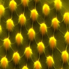
An enlarged image shows semiconductor material stretched to enhance its electronic potential to catch solar energy. Credit: Hong Li/Stanford University |
Stanford University's Energy department is on the forefront of developing new energy technologies, and their latest is a crystal used for solar cells. The technology is similar to semiconductors used in the electronics industry.
"To make semiconductors useful, engineers must tweak their crystalline lattice in subtle ways to start and stop the flow of electrons," the researchers explained. "Semiconductor engineers must know precisely how much energy it takes to move electrons in a crystal lattice."
Semiconductor materials, like silicon, gallium arsenide, and germanium, each have a band gap unique to their crystalline lattice, which is the energy measure of the material. The researchers explained that "this energy measure helps determine which material is best for which electronic task."
The development by the Stanford researchers is a semiconductor crystal with a variable band gap -- which could lead to solar cells that are more sensitive to a broader spectrum of light, and therefore can absorb more energy from the sun. The researchers, Stanford mechanical engineer Xiaolin Zheng and physicist Hari Manoharan, published their findings in Nature Communications, and explained that, even though the material -- Molybdenum disulfide, or MoS2 -- is not new -- it has some electronic properties that derive from how this crystal forms its lattice.
"From a mechanical engineering standpoint, monolayer MoS2 is fascinating because its lattice can be greatly stretched without breaking," said Zheng in a statement.
The researchers stretched this lattice to shift atoms in the monolayer -- which created an artificial crystal with a variable band gap.
"With a single, atomically thin semiconductor material we can get a wide range of band gaps," Manoharan said. "We think this will have broad ramifications in sensing, solar power and other electronics."
MoS2 has benefits beyond just absorbing additional light -- it is also fairly inexpensive to produce, which could lead to further innovation on artificial crystals. Stanford's study builds upon one that was conducted by MIT last year.
"One of the most exciting things about our process is that is scalable," Zheng said. "From an industrial standpoint, MoS2 is cheap to make."
Although solar technologies are evolving, the gap between university and real-life use is still a wide one. According to Ken Johnson with the Solar Energy Industries Association (SEIA), innovation in education doesn't always mean the industry will jump on board -- at least not immediately.
"Clearly, both [universities and utilities] have a part to play [in innovation], but this report is missing a critical link between the two," Johnson told FierceEnergy. "Technology doesn't often flow directly from universities to utilities, and regulated utilities aren't, for the most part, natural innovators because of the scope of their allowed activities."
Johnson added that "a more likely path is for technology to be spun out of a university to existing or startup companies, who then do the work to commercialize the technology by figuring out scaled manufacturing, developing a business model and selling the technology to utilities -- or even bypassing the utilities and selling directly to end customers."
For more:
- visit this
website
© 2015 FierceMarkets, a division of Questex, LLC. All rights reserved.